Making FAB IPS Board
FAB IPS Board Helps to program microcontrollers on different boards
Steps I used to make my electronics production exercise (production of A FAB IPS):
1. I downloaded the AVR studio 6 software from the internet and I installed it on my computer
2.To make the FabISP circuit programmer I go to the following link on the fablab schedule
page:“http://fab.cba.mit.edu/content/projects/fabisp/“
prepared by David. From this page I got all the materials I need to manufacture
my circuit board: schematics, FABISP.png, firmware.zip, etc
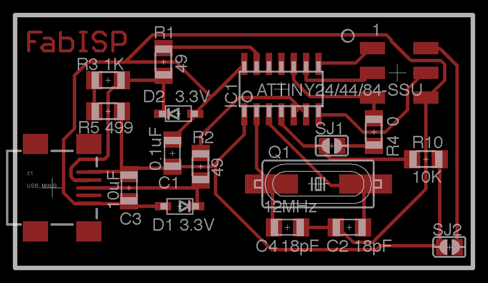
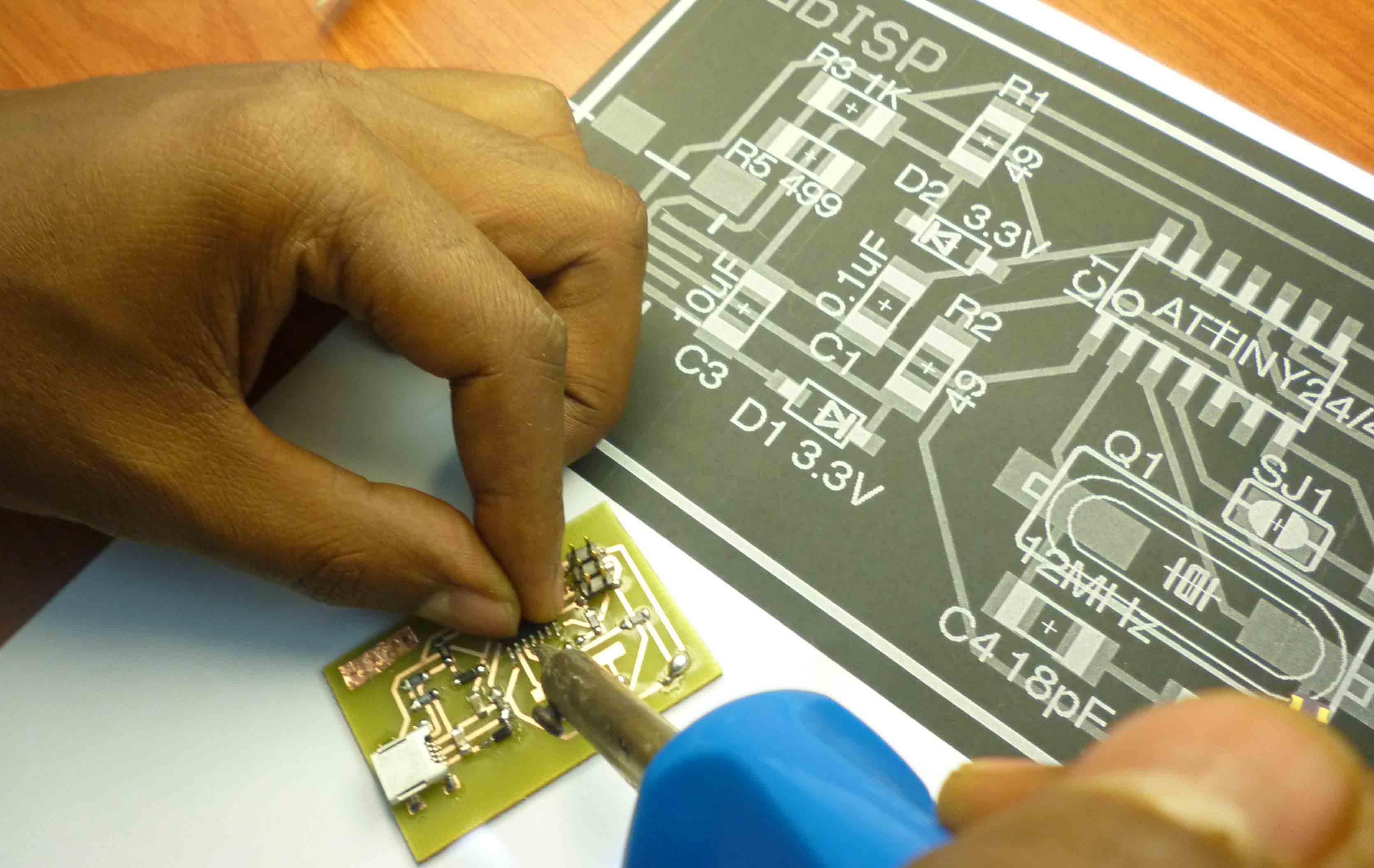
3.I learn what components I need to produce the FABISP board. And the components are:
two 3.3 volt zener diode, two 49 ohm resistors, one 499 ohm resistor, one 0 ohm resistor,
one 10 kilo resistor, one 1 kilo resistor,two 18 Pico farad capacitors, one 10 micro farad capacitor,
one 0.1 micro farad capacitor, one 12 mega herze crystal, Two jumpers, Tiny USB connector, one 6-pin
ISP header, one tiny 44 microcontroller, AVR ISP mkII Main and cables.
As shown on the following picture:
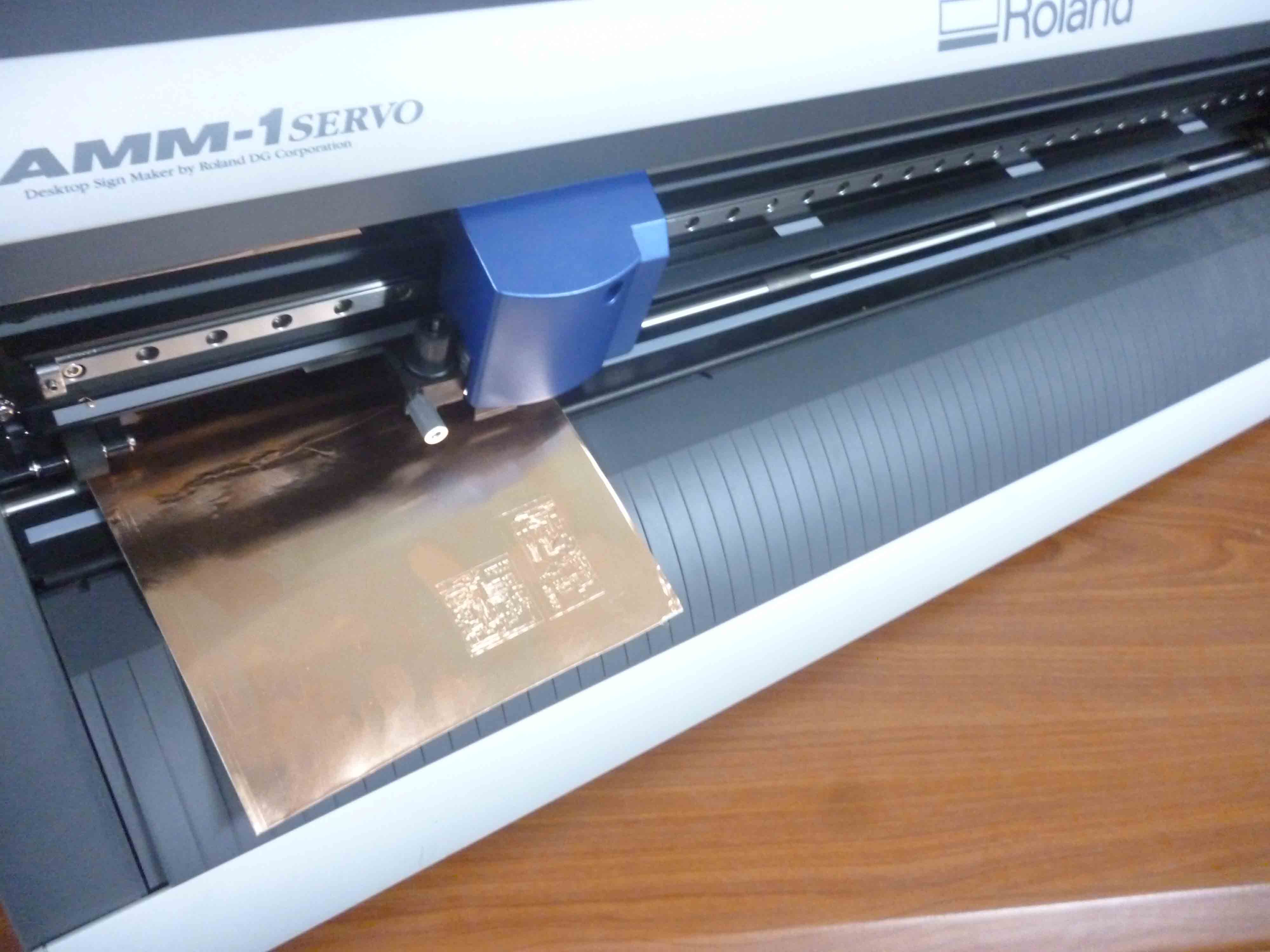
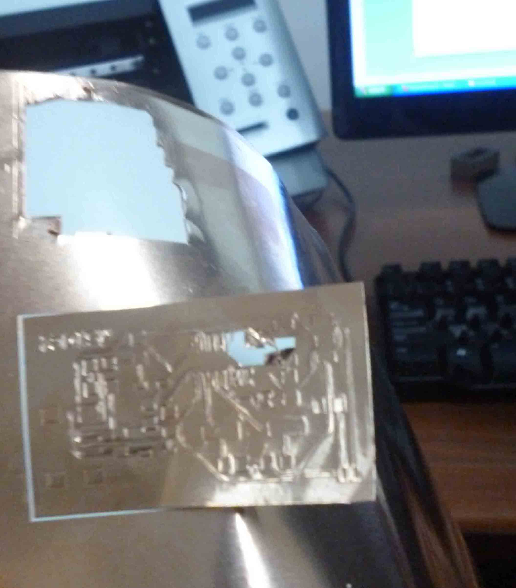
 4.we made an attempt to mile the board with our Modella machine but it was not working.
The second attempt was to make the board by printing on a copper paper by making use of the
Roland vinyl cutter. But as we could not quite make this one work either because the print out
(the lay out) was too small for the cutter, we were forced to think of other options.
More trouble shooting was needed but we thought it would not work out with our schedule.
I will make sure to debug the issue in the future. See the following picture:
4.we made an attempt to mile the board with our Modella machine but it was not working.
The second attempt was to make the board by printing on a copper paper by making use of the
Roland vinyl cutter. But as we could not quite make this one work either because the print out
(the lay out) was too small for the cutter, we were forced to think of other options.
More trouble shooting was needed but we thought it would not work out with our schedule.
I will make sure to debug the issue in the future. See the following picture:
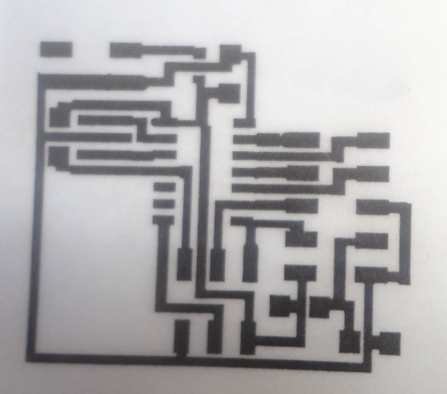
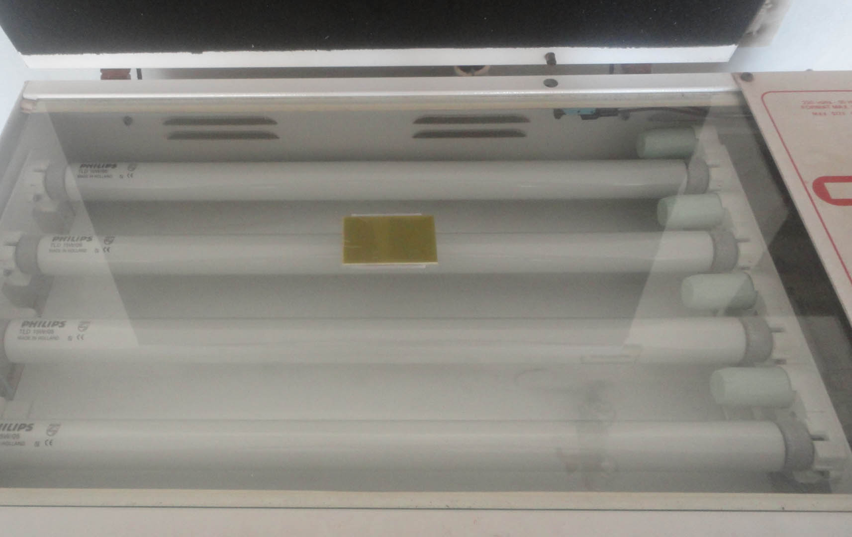
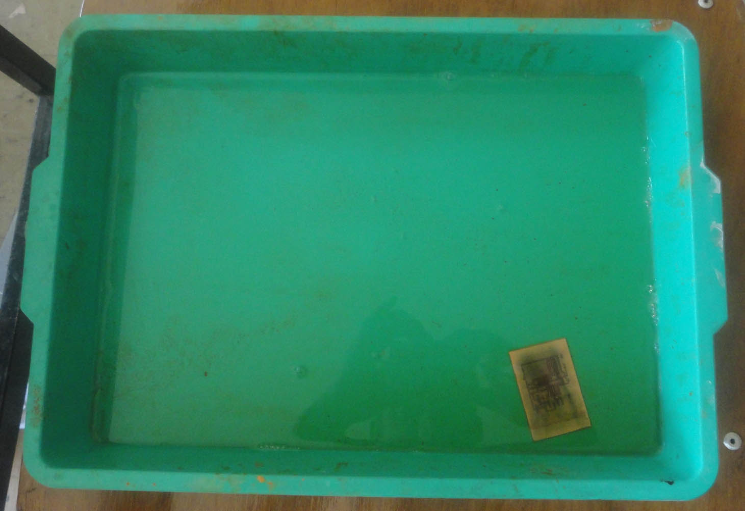
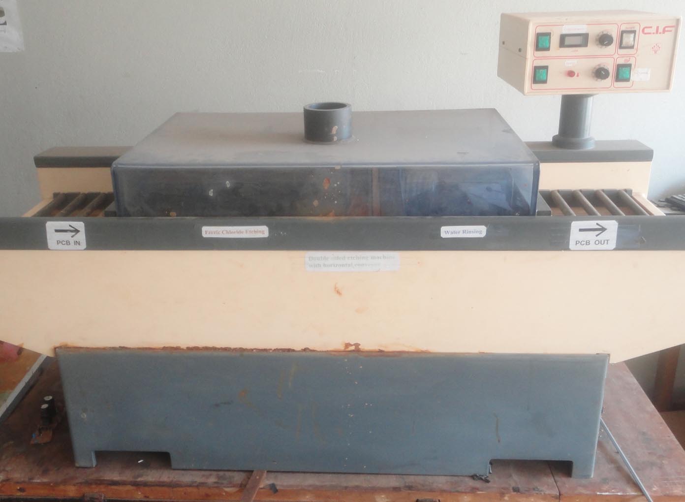
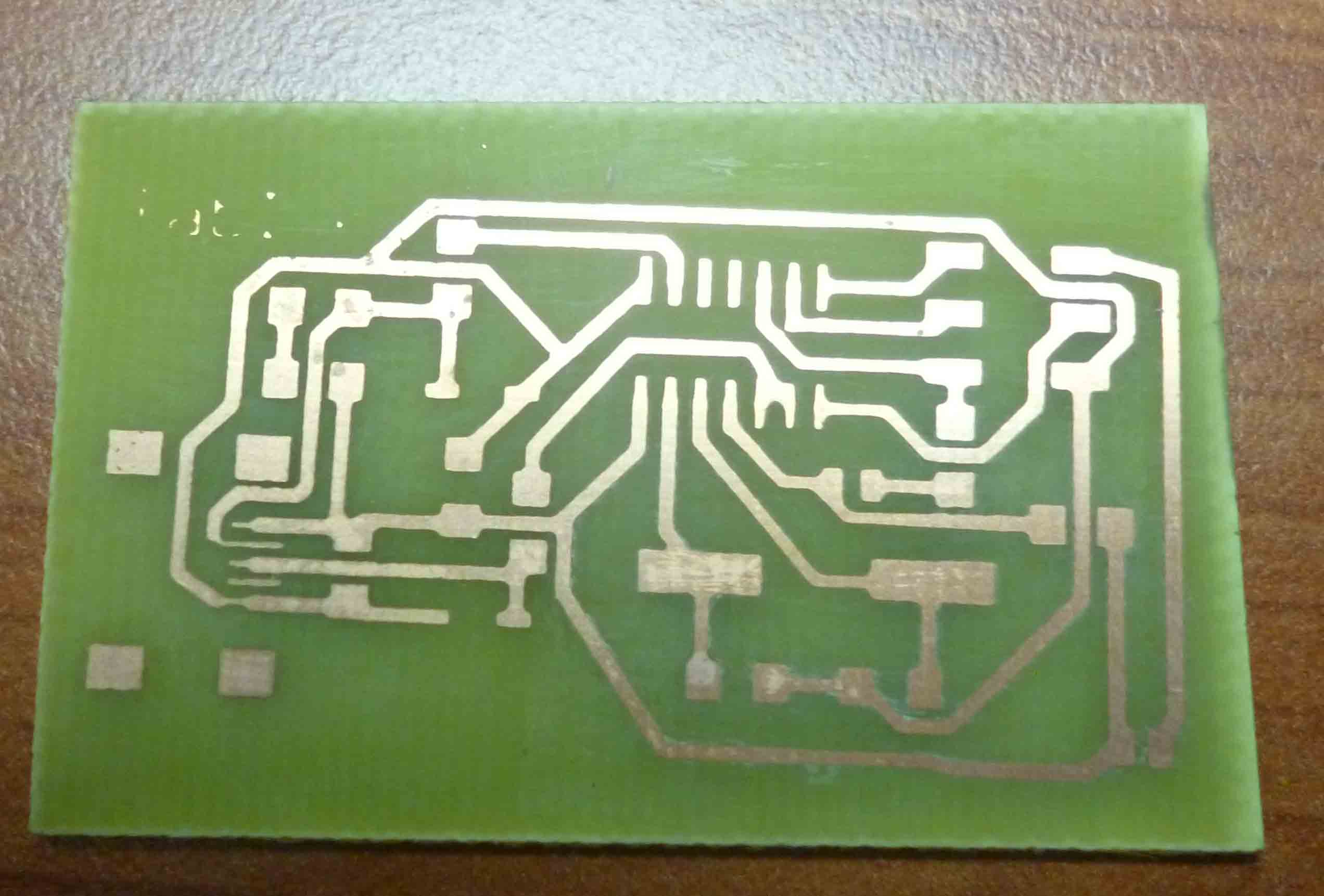
 5. the other option: Using UV exposure and ferric-chloride etching to make the PCB ISP.
The following are the steps are important to prepare a board by chemicals:
a. prepare the drawing on eagle
b. modify the drawing (lay out)
c. print the lay out on a transparent paper
   (or tracing paper)
d. place the lay out on a copper coated board
   and expose it to UV light in a UV light box for five minuts
e. remove the transparent paper and bath the board
   in dilute sodium hydroxide
f. put the board in an etching machine
see the following pictures for illustration :
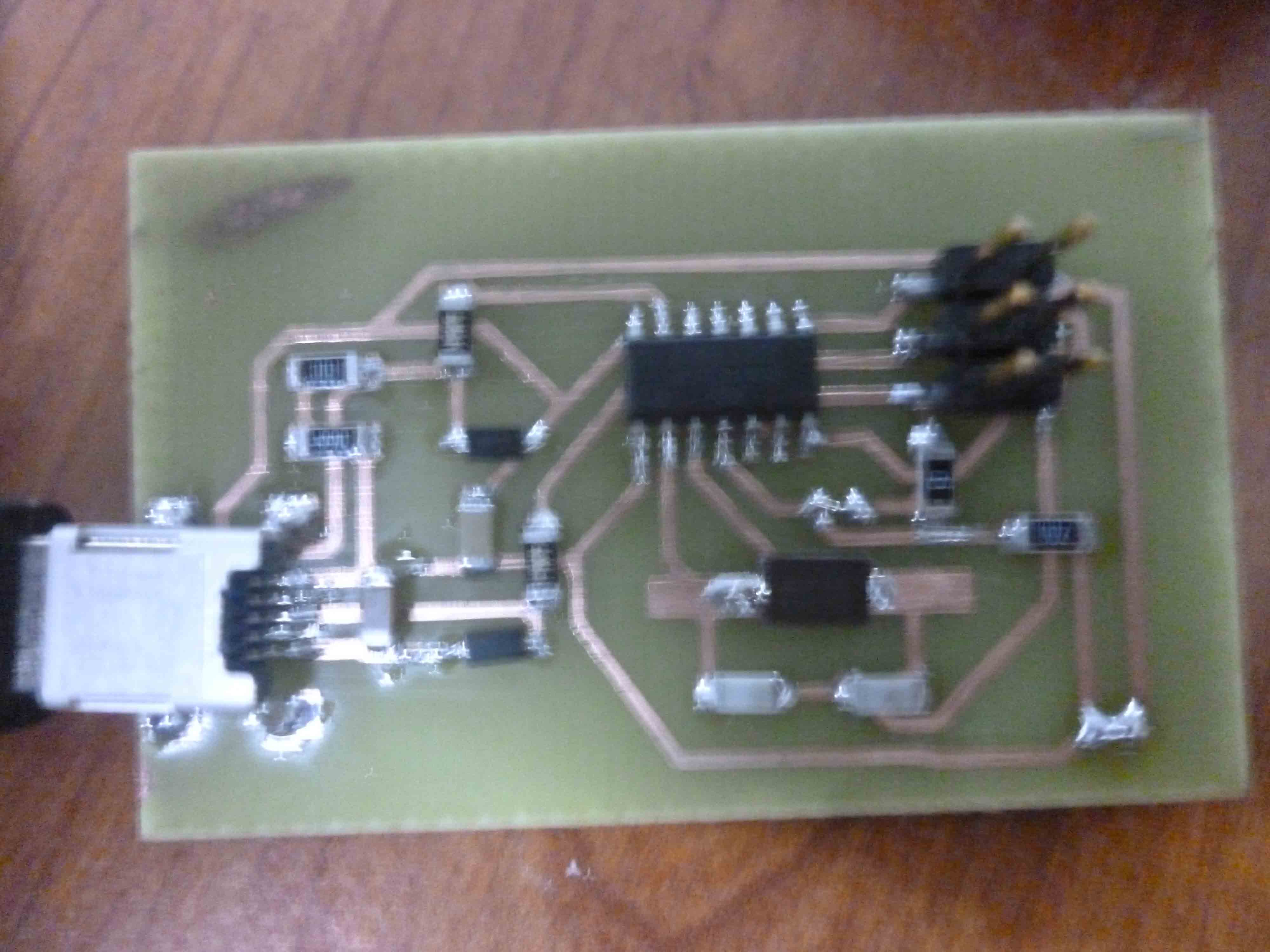
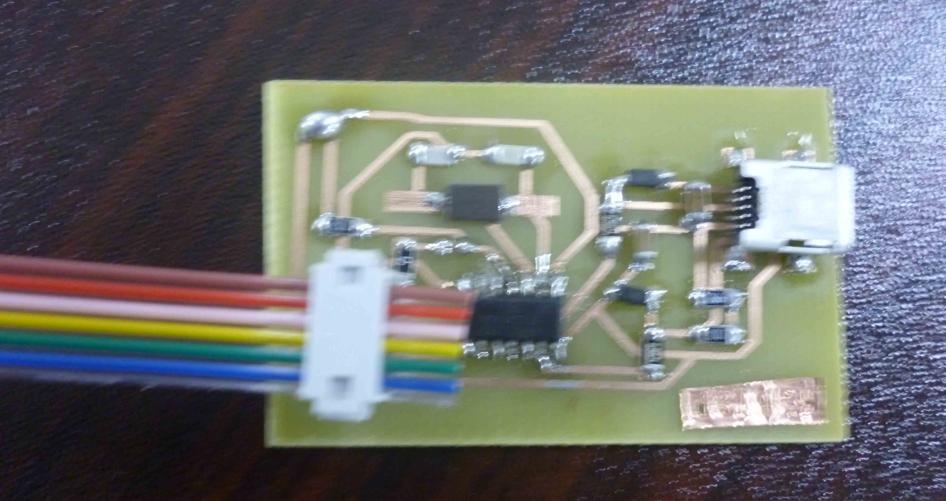
 6. soldering the components:
Here one should be careful to check on the directions of the diodes,
the direction of the head of the tiny 44. See the following pictures:
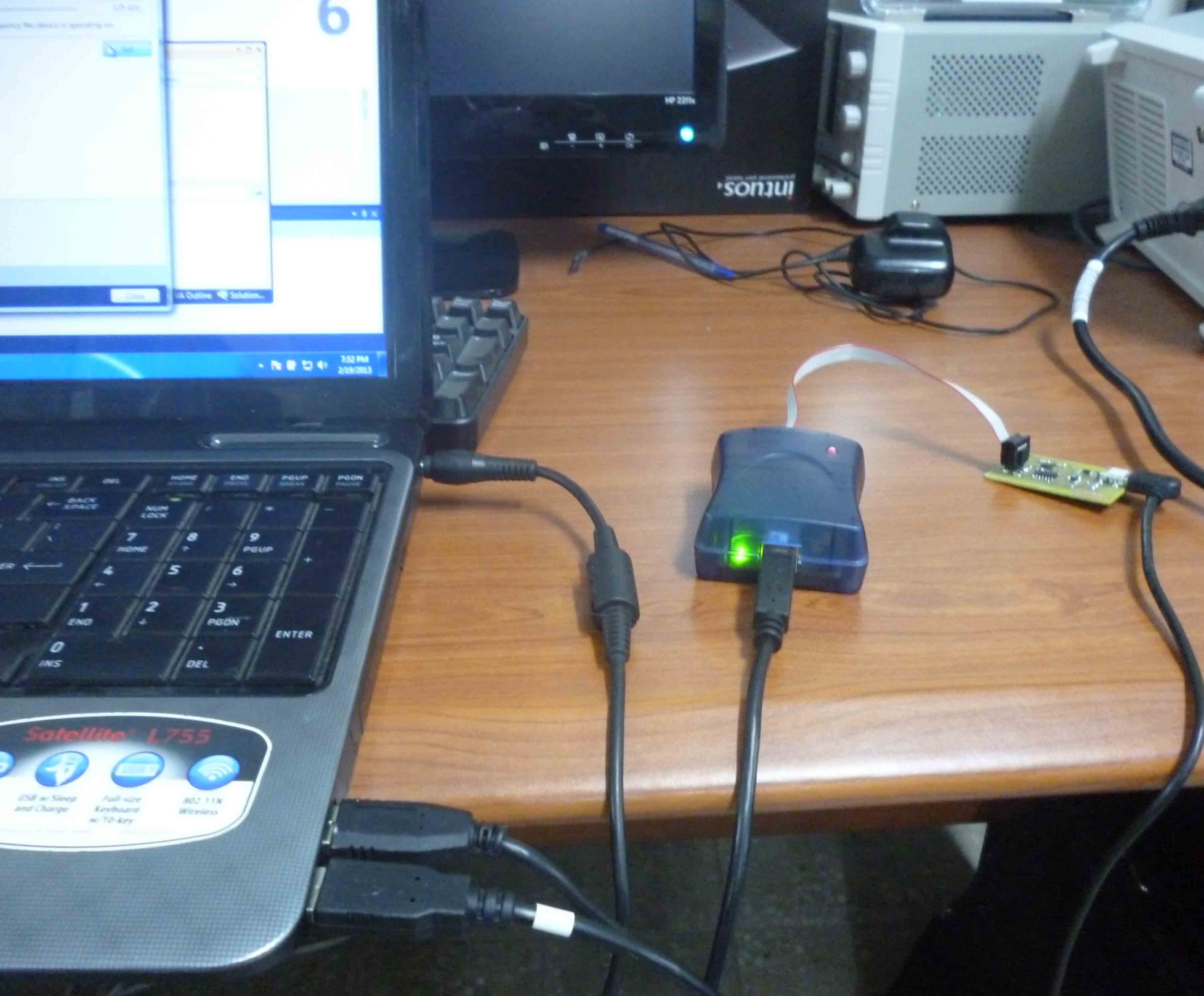
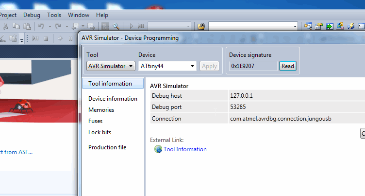
 7. now it is time to program our micro controller by using AVR studio software and AVR mkII.
See this link for more elaboration by David “http://fab.cba.mit.edu/content/projects/fabisp/”.
I used the former link as a guide to perform my exercise: see the following pictures:
7. now it is time to program our micro controller by using AVR studio software and AVR mkII.
See this link for more elaboration by David “http://fab.cba.mit.edu/content/projects/fabisp/”.
I used the former link as a guide to perform my exercise: see the following pictures:
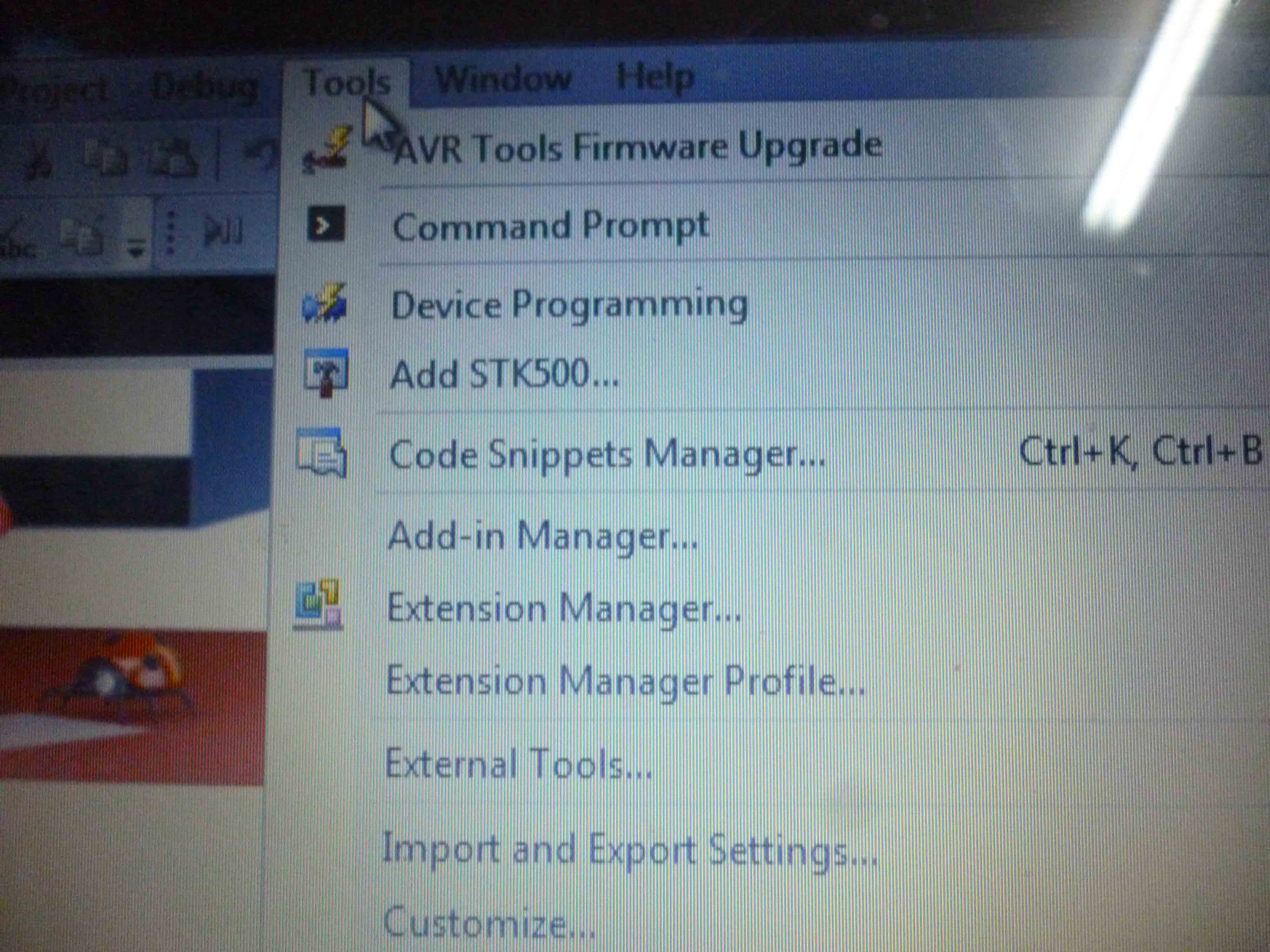
On the next step AVR studio 6 recognized my board with device signature 0x1E9207
The remaining steps are to write the program to the baord by making use of david's 'makefile' from the 'firmware.zip' . . .
